InP

Indium Phosphide Wafer Finishing

Drawing-specific handling and protected surface contact for high-value compound-semiconductor substrates.
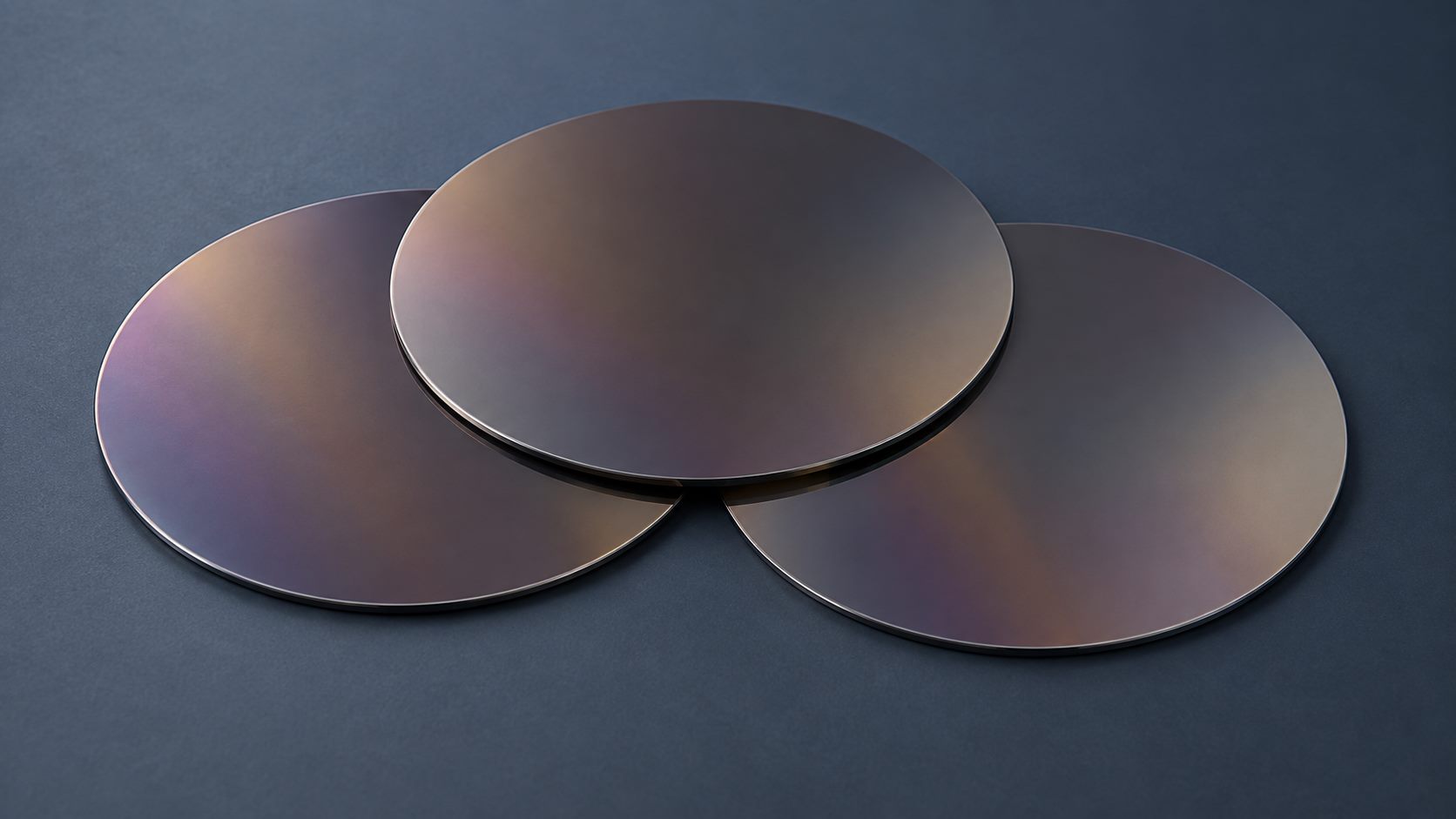
Application visual: InP material blanks
Application material visual

APPLICATION

Indium Phosphide Wafer Finishing

  • Fragile-edge and surface protection
  • Controlled handling
  • Chemistry-aware finishing

PRODUCT AVAILABILITY

Custom products for the application.

  • Multiple product families
  • Custom materials and dimensions
  • Quotation from drawing, sample or requirement

SUPPLY SUPPORT

From samples to repeat orders.

  • Global quotation support
  • Sample and project communication
  • Repeat-order supply

AVAILABLE PRODUCT TYPES

Products that may suit this application.

Final material, dimensions and configuration are confirmed for the order.
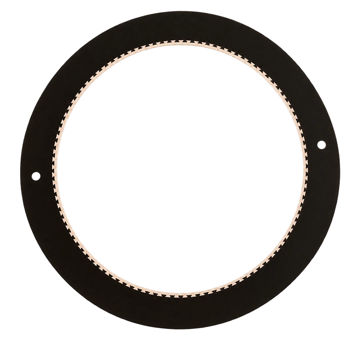
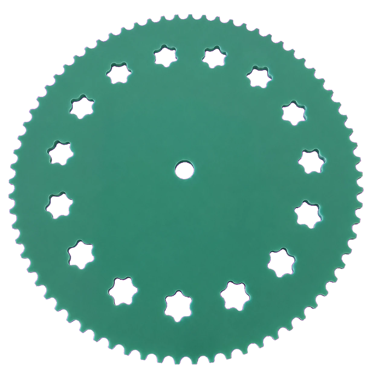
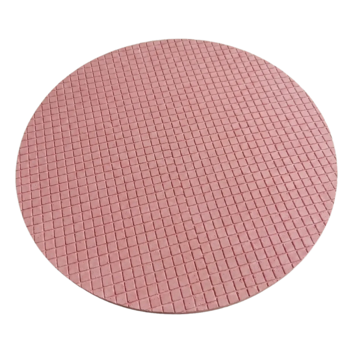
NWS-PAD-2302NWS-PAD-2302 Nonwoven Wafer Pre-Polishing PadsNonwoven Wafer Pre-Polishing Pads for sic, gaas, silicon, sapphire and metal. Initial polishing. Thickness: 0.8–4.0 mm; Hardness: Shore A 35–92. Custom-made for the agreed process.View product →NWS-PAD-2303NWS-PAD-2303 Compliant Final-Polishing ClothCompliant Final-Polishing Cloth for sic, gaas, silicon, sapphire and glass. Final polishing. Thickness: 0.5–2.0 mm; Hardness: Shore A 32–65. Custom-made for the agreed process.View product →NWS-PAD-2501NWS-PAD-2501 Synthetic-Fibre Pads for Wafer LappingSynthetic-Fibre Pads for Wafer Lapping for sic, gan, gaas, inp, silicon and optical glass. Lapping / polishing. Typical thickness: 1.30 mm; Typical density: 0.43 g/cm³. Custom-made for the agreed process.View product →NWS-HLD-2101NWS-HLD-2101 Waxless Wafer Support PadsWaxless Wafer Support Pads for silicon, sapphire and compound-semiconductor wafers. Wafer holding. Typical thickness: 0.58 mm; Typical density: 0.57 g/cm³. Custom-made for the agreed process.View product →NWS-POL-3402NWS-POL-3402 Fine Alumina Slurry for Compound SemiconductorsFine Alumina Slurry for Compound Semiconductors for compound-semiconductor workpieces. Fine polishing. Abrasive: Aluminum oxide; Particle-size range: 0.05–0.8 µm across grades. Custom-made for the agreed process.View product →NWS-POL-3602NWS-POL-3602 Alumina Slurry for InP Pre-PolishingAlumina Slurry for InP Pre-Polishing for indium phosphide workpieces. Coarse polishing. Abrasive: Aluminum oxide; Particle-size reference: 0.561 µm. Custom-made for the agreed process.View product →NWS-POL-3603NWS-POL-3603 Silica Slurry for InP Fine PolishingSilica Slurry for InP Fine Polishing for indium phosphide workpieces. Fine polishing. Abrasive: Colloidal silica; Particle-size reference: 103.3 nm. Custom-made for the agreed process.View product →Composite carrierMetal-Body Carriers with Polymer InsertsA rigid metal drive body with replaceable or integrated polymer contact zones around sensitive workpieces.View product →Protected contactEdge-Protection Composite CarriersComposite pocket interfaces developed for thin, brittle or high-value substrates where edge contact is the primary risk.View product →Engineering polymerPEEK, PI, PPS & PEI Carrier DirectionsEngineering-polymer carrier directions screened around temperature, chemistry, stiffness, wear and workpiece contact.View product →Low-hardness plateGlass Lapping PlatesPlain or grooved glass-plate directions for selected softer compound-semiconductor and optical finishing routes.View product →

APPLICATION QUOTATION

Send the product name, drawing or sample photo.

Request a quote →

WORKPIECE & PROCESS FIT

InP, GaAs and GaN substrate finishing

Indium phosphide, gallium arsenide and gallium nitride substrates.
What to specify
Crystal orientation, doping, dimensions, fragility and process chemistry. Define substrate finishing separately from epitaxial or patterned surfaces.
Made-to-order consumables
Carrier geometry and material, plate grooves, pad contact properties, conditioning, cleaning and polishing media are reviewed for the actual process. Drawing review and first-article support establish the repeat-order specification.