
APPLICATIONS
Start with the material you need to finish.
Find the closest workpiece below. Each page explains the main surface risks and what we would need to check before recommending a carrier, pad, plate or slurry. Images illustrate materials; they do not show supplied customer parts.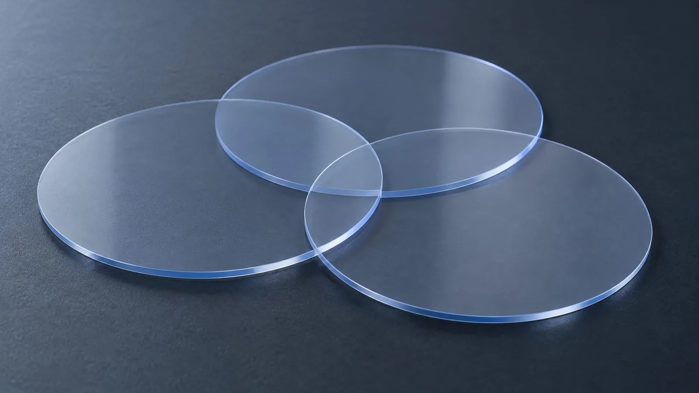
Al₂O₃ · Sapphire
Sapphire Wafer Finishing
A hard, brittle substrate route connecting edge protection, removal rate, plate or pad choice and final surface control.Explore the application route →02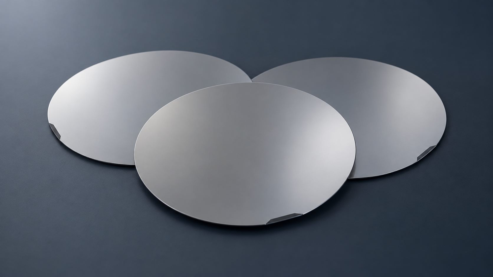
Si · Silicon
Silicon Wafer Finishing
Machine-matched workholding and chemistry-aware contact for controlled single- or double-side wafer finishing.Explore the application route →03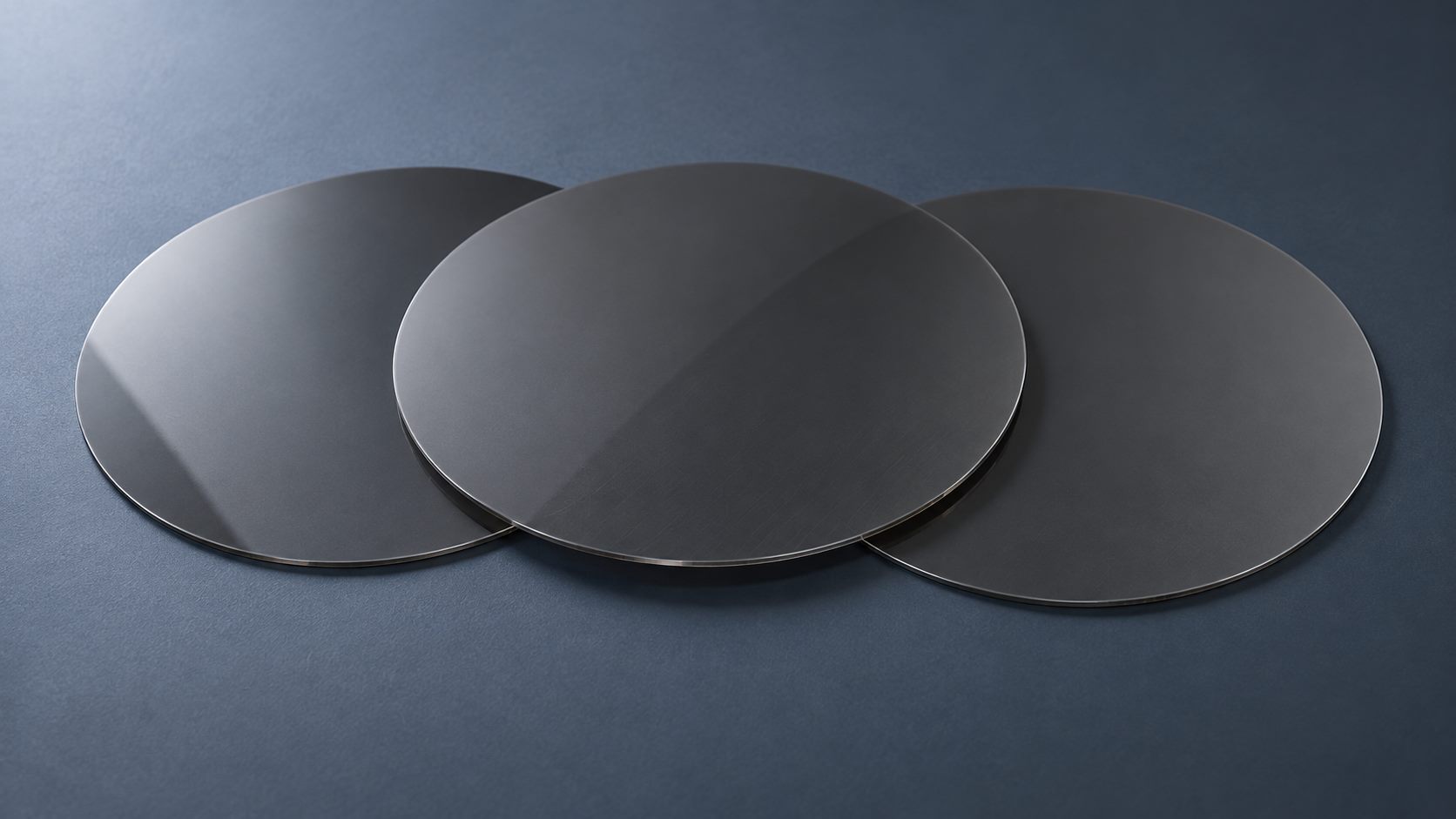
SiC
Silicon Carbide Substrate Finishing
A hard-material programme that aligns carrier, plate, diamond abrasive, cleaning and inspection around the required surface.Explore the application route →04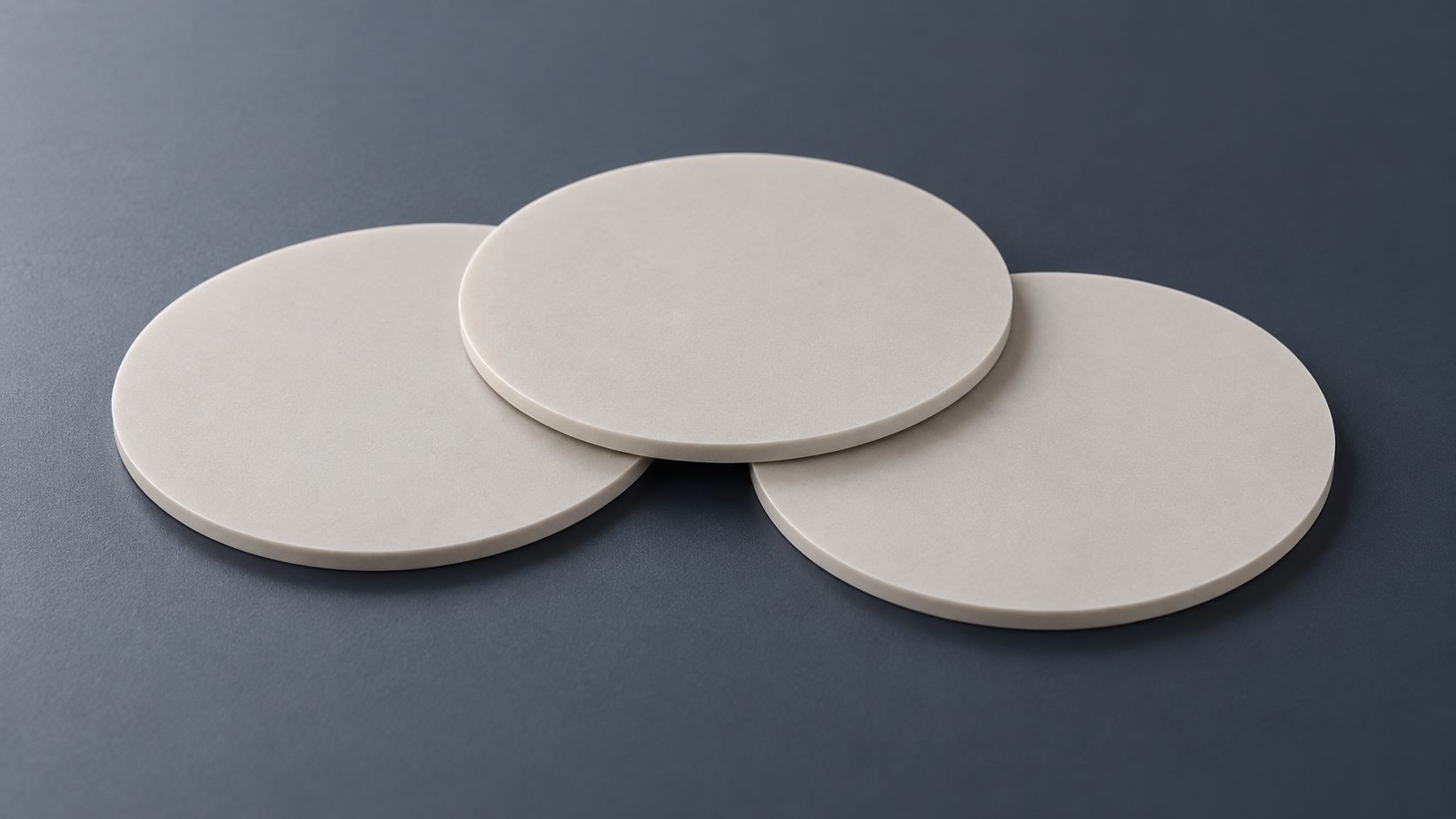
AlN
Aluminum Nitride Ceramic Finishing
Stable support and contamination-aware wet finishing for thin thermal and electronic ceramic substrates.Explore the application route →05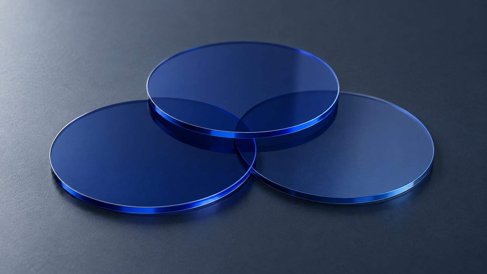
Blue Glass
Blue Glass Optical Filter Finishing
Contact control and stable slurry transport for sensitive optical-filter substrates.Explore the application route →06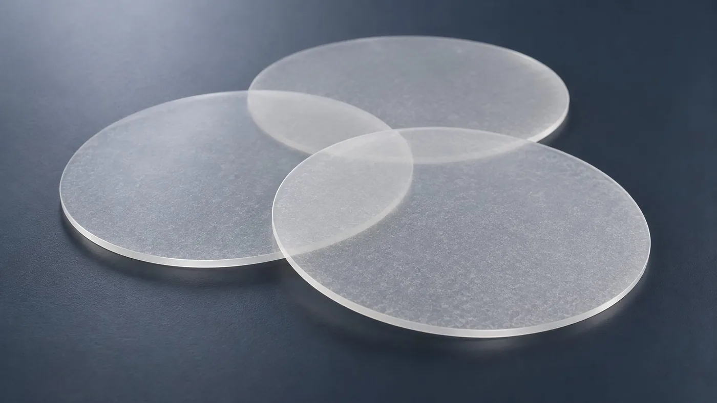
Microglass
Microcrystalline Glass Wafer Finishing
A precision-glass route balancing pocket clearance, thickness control, edge risk and target finish.Explore the application route →07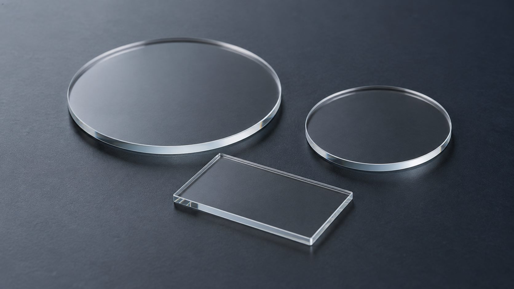
Optical Glass
Optical Glass Finishing
Application-specific pads, compounds and tooling for planar or shaped optical surfaces.Explore the application route →08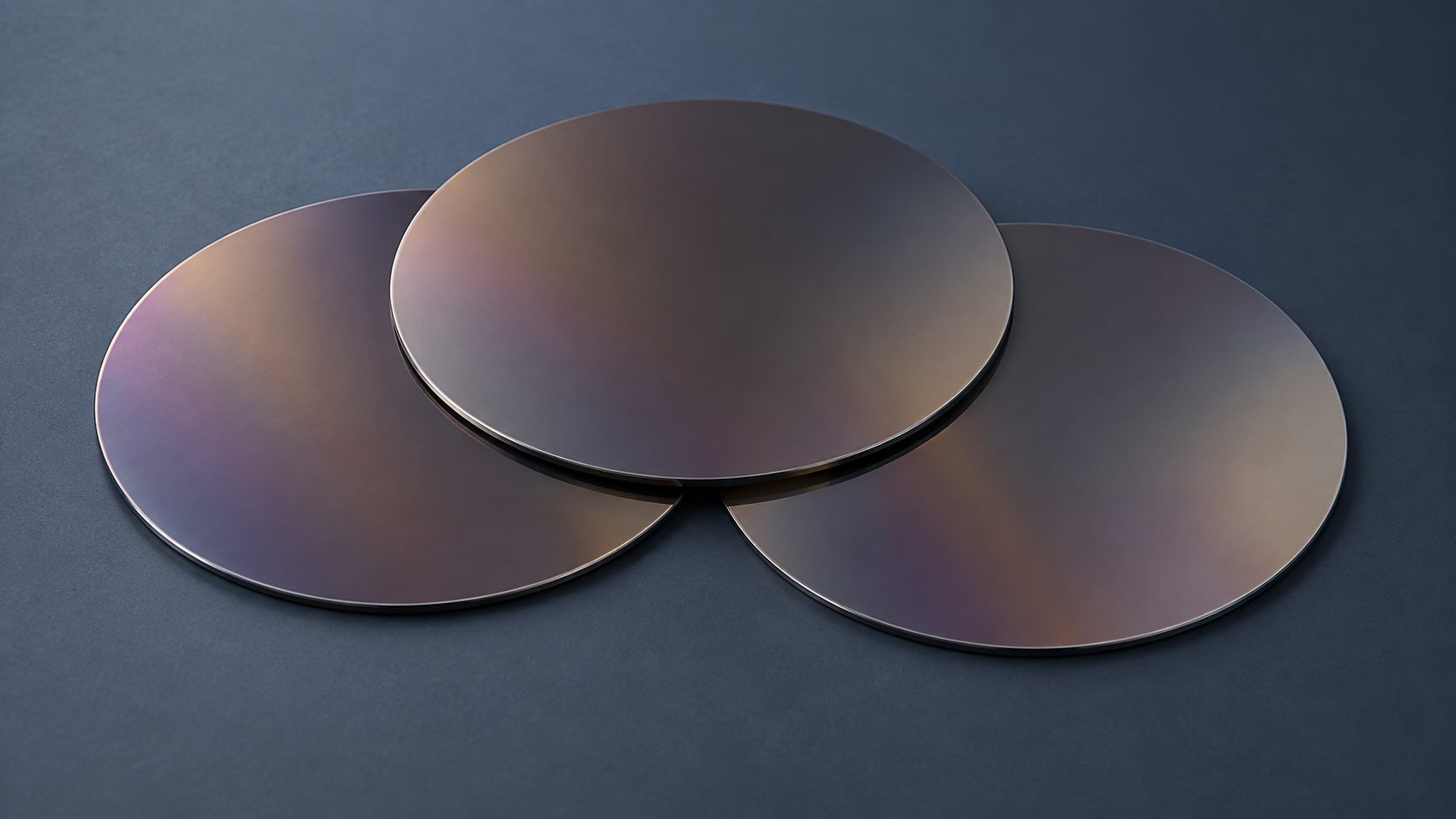
InP
Indium Phosphide Wafer Finishing
Drawing-specific handling and protected surface contact for high-value compound-semiconductor substrates.Explore the application route →09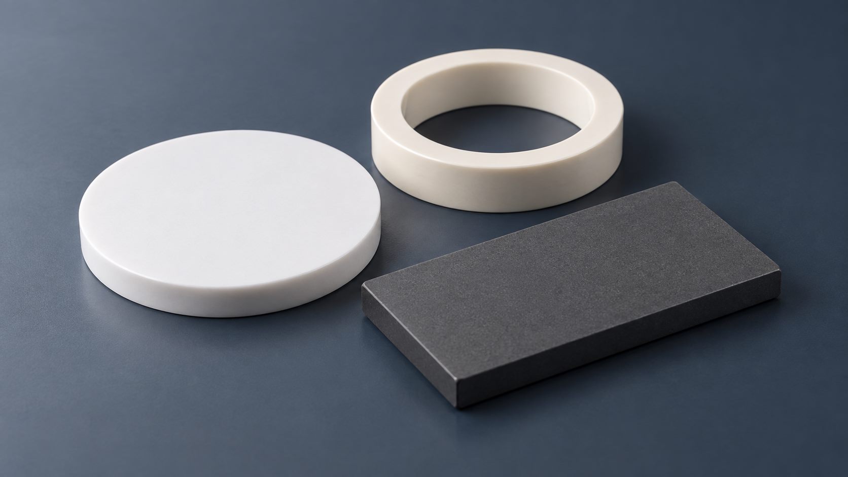
Al₂O₃ · ZrO₂ · SiC
Technical Ceramic Component Finishing
A material-specific route for hard, brittle ceramic parts that connects stock removal, edge control, plate condition and final inspection.Explore the application route →10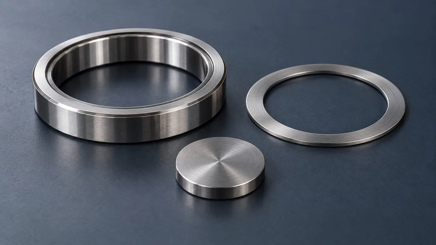
Steel · Alloy · Bearing
Precision Metal & Bearing Component Finishing
Flatness, parallelism and surface-control routes for seals, bearing parts, hydraulic components and other precision metal workpieces.Explore the application route →11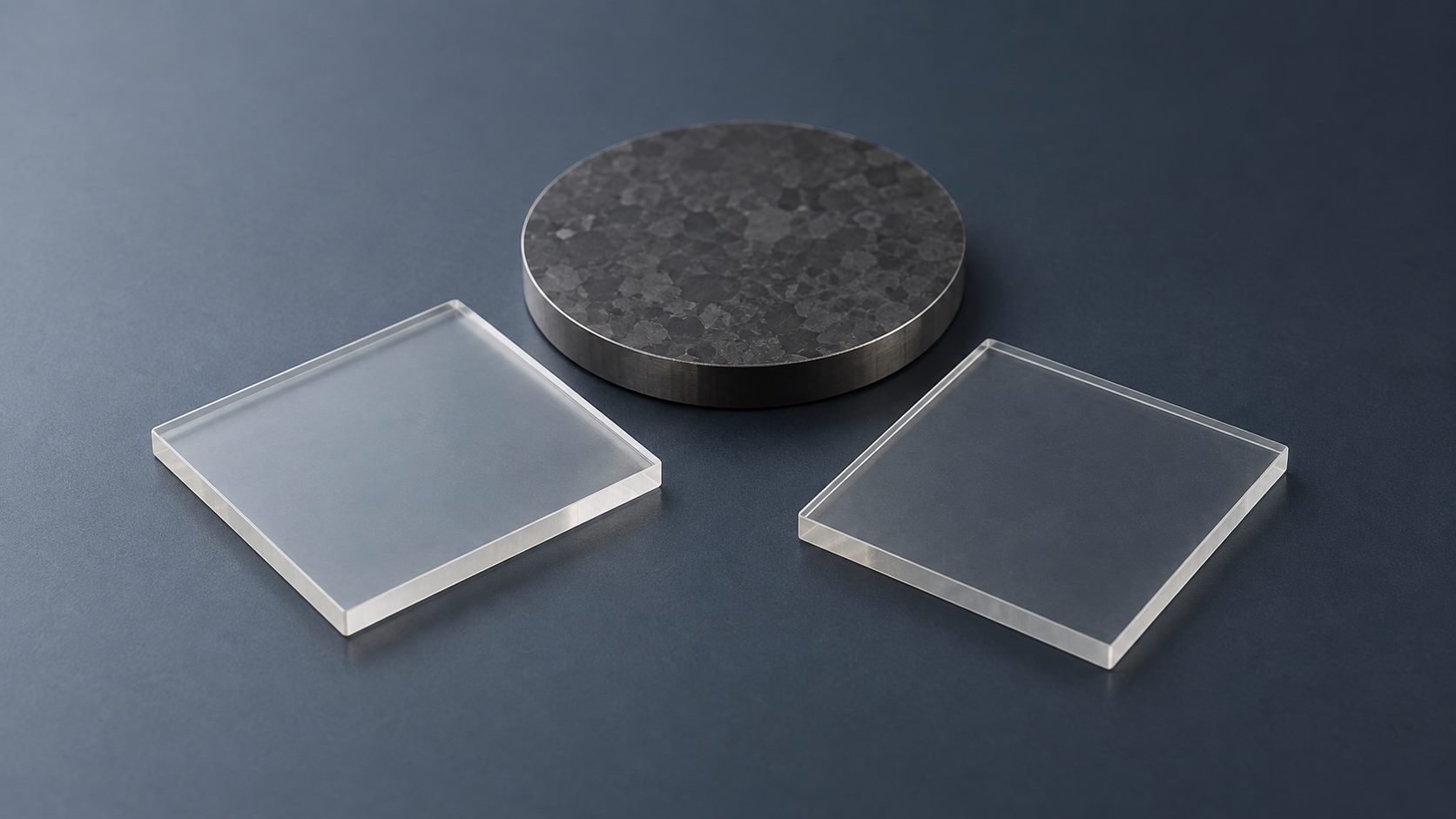
Diamond · CVD
Diamond & CVD Component Finishing
A staged lapping and polishing review for hard diamond components, tools and CVD blanks without confusing grinding, lapping and final polishing.Explore the application route →12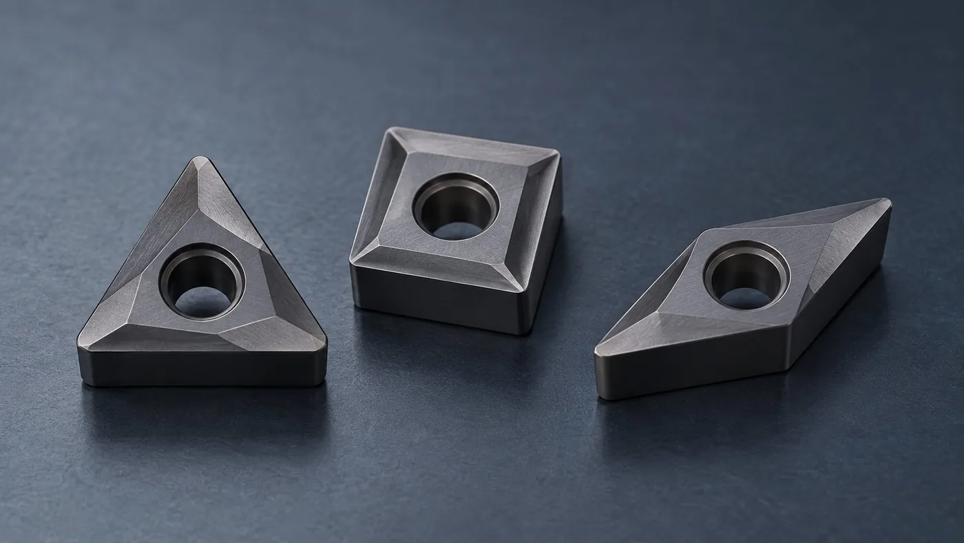
WC-Co · Cermet · CBN/PCD